讨论出处:链接
My questrion is similar with that in 链接, but I am still misunderstanding with something.
Chip: AM33359 (Beaglebone Version A6)
OS:Linux 3.2
I am sending data from an FPGA by using the GPMC bus(CS1). My configuration:
[    1.121124] GPMC_CONFIG1:e8001001    //Burst, sync, 8-bit, non multiplexed, Nor device, FCLK/2
[    1.124572] GPMC_CONFIG2:00181800
[    1.128051] GPMC_CONFIG3:22181810
[    1.131500] GPMC_CONFIG4:18007818
[    1.134948] GPMC_CONFIG5:000a1818
[    1.138427] GPMC_CONFIG6:8e060000
[    1.141876] GPMC_CONFIG7:00000f01    // CS1
gpmc timing setting:


#define GPMC_FPGA_SYNC_CLK_NS   (20)
static struct gpmc_timings aplus_fpga_timings = {
    /* Minimum clock period for synchronous mode (in picoseconds) */
    .sync_clk = 1000 * GPMC_FPGA_SYNC_CLK_NS, /* 10ns */
    .cs_on = 0,
    .cs_rd_off = 12 * GPMC_FPGA_SYNC_CLK_NS,       /* Read deassertion time */
    .cs_wr_off = 12 * GPMC_FPGA_SYNC_CLK_NS,       /* Write deassertion time */
    /* ADV signal timings corresponding to GPMC_CONFIG3 */
    .adv_on = 0,            /* Assertion time */
    .adv_rd_off = 12 * GPMC_FPGA_SYNC_CLK_NS,       /* Read deassertion time */
    .adv_wr_off = 12 * GPMC_FPGA_SYNC_CLK_NS,       /* Write deassertion time */
    /* WE signals timings corresponding to GPMC_CONFIG4 */
    .we_on = 0 * GPMC_FPGA_SYNC_CLK_NS,        /* WE assertion time */
    .we_off = 12 * GPMC_FPGA_SYNC_CLK_NS,      /* WE deassertion time */
    /* OE signals timings corresponding to GPMC_CONFIG4 */
    .oe_on = 4 * GPMC_FPGA_SYNC_CLK_NS,        /* OE assertion time */
    .oe_off = 12 * GPMC_FPGA_SYNC_CLK_NS,      /* OE deassertion time */
    /* Access time and cycle time timings corresponding to GPMC_CONFIG5 */
    .page_burst_access = 1 * GPMC_FPGA_SYNC_CLK_NS,    /* Multiple access word delay */
    .access = 5 * GPMC_FPGA_SYNC_CLK_NS,       /* Start-cycle to first data valid delay */
    .rd_cycle = 12 * GPMC_FPGA_SYNC_CLK_NS,        /* Total read cycle time */
    .wr_cycle = 12 * GPMC_FPGA_SYNC_CLK_NS,        /* Total write cycle time */
    /* The following are only on OMAP3430 */
    .wr_access = 7 * GPMC_FPGA_SYNC_CLK_NS,        /* WRACCESSTIME */
    .wr_data_mux_bus = 3 * GPMC_FPGA_SYNC_CLK_NS,  /* WRDATAONADMUXBUS */
};
I have a 8-bit counter inside the FPGA incrementing with the falling edge of the gpmc_clk.In this way, data are sending to the ARM on the rising edge of the gpmc_clk and they change (from the FPGA side) on the falling edge of the clock. linux read driver is simple as below:
1
2
3
4
    static void omap_read_buf8(struct omap2_aplus_fpga_dev *fpga_dev, u_char *buf, int len)
    {
        ioread8_rep((void __iomem *)fpga_dev->virt_base, buf, len);
    }
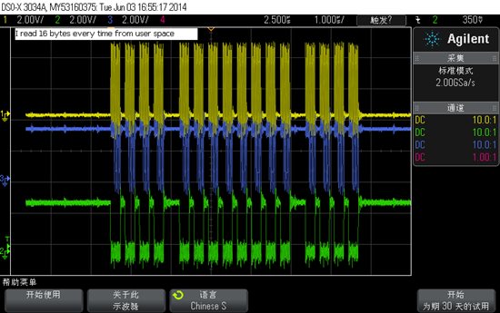
When I read 16 bytes every time from user space programme, it just retured:
1
2
3
4
5
6
7
8
9
    ...
    [  264.266845] aplus_fpga read count 16
    [  264.279724] aplus_fpga read 16, fpga_phys_base 01000000,virt_base d1000000
    read buf conrtent:
    1 1 11 11 21 21 31 31 41 41 51 51 61 61 71 71
    [  269.292388] aplus_fpga read count 16
    [  269.305419] aplus_fpga read 16, fpga_phys_base 01000000,virt_base d1000000
    read buf conrtent:
    81 81 91 91 a1 a1 b1 b1 c1 c1 d1 d1 e1 e1 f1 f1
Waves on the oscilloscope in attachments.
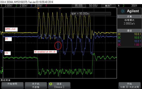
wave of each read cycle
Qeustion 1: No matter I set the device width 8 or 16bits, burst or single mode, it just the same result. “8-bit wide devices are supported only in single synchronous or single asynchronous read or write mode”(Please see section 7.1.3.3 in the AM335X TRM Rev.I).It makes me wonder.
Question 2:I can’t get “1 2 3 4 5 6 7 8 9 a b c d e f…” as excepted but “1 1 11 11 21 21 31 31 41 41 51 51 61 61 71 71” indeed.It seems that I can only read the first byte and other 7 bytes lost during every read cycle(with 12 gpmc_clk,oe assert on 4th gpmc_clk, 8 bytes output), why? Is my linux driver programme wrong?
Posted by Biser Gatchev-XID on Jun 03 2014 08:02 AM
Q1: The TRM is correct. For 8-bit devices burst mode is not supported. Q2: Have you verified that the FPGA outputs data correctly?
Posted by yi xiaoyang on Jun 03 2014 21:23 PM
Q1:TRM is right,I think I haven’t test burst mode clearly.
Q2:You’are right! FPGA has one bit error, I checked it carefully, It seems that there is cold solder join on D3 pin. But what’s more, the FPGA output depend on the GPMC timing configuration.Is works all right with bellow timing.
Thank you very much,You helped me~
1
2
3
4
5
6
7
8
9
10
11
12
13
14
15
16
17
18
19
20
21
22
23
24
25
    static struct gpmc_timings aplus_fpga_timings = {
       /* Minimum clock period for synchronous mode (in picoseconds) */
       .sync_clk = 1000 * GPMC_FPGA_SYNC_CLK_NS, /* 10ns */
       .cs_on = 0,
       .cs_rd_off = 2 * GPMC_FPGA_SYNC_CLK_NS,       /* Read deassertion time */
       .cs_wr_off = 2 * GPMC_FPGA_SYNC_CLK_NS,       /* Write deassertion time */
       /* ADV signal timings corresponding to GPMC_CONFIG3 */
       .adv_on = 0,            /* Assertion time */
       .adv_rd_off = 6 * GPMC_FPGA_SYNC_CLK_NS,       /* Read deassertion time */
       .adv_wr_off = 6 * GPMC_FPGA_SYNC_CLK_NS,       /* Write deassertion time */
       /* WE signals timings corresponding to GPMC_CONFIG4 */
       .we_on = 0 * GPMC_FPGA_SYNC_CLK_NS,        /* WE assertion time */
       .we_off = 6 * GPMC_FPGA_SYNC_CLK_NS,      /* WE deassertion time */
       /* OE signals timings corresponding to GPMC_CONFIG4 */
       .oe_on = 0 * GPMC_FPGA_SYNC_CLK_NS,        /* OE assertion time */
       .oe_off = 1 * GPMC_FPGA_SYNC_CLK_NS,      /* OE deassertion time */
       /* Access time and cycle time timings corresponding to GPMC_CONFIG5 */
       .page_burst_access = 1 * GPMC_FPGA_SYNC_CLK_NS,    /* Multiple access word delay */
       .access = 1 * GPMC_FPGA_SYNC_CLK_NS,       /* Start-cycle to first data valid delay */
       .rd_cycle = 2 * GPMC_FPGA_SYNC_CLK_NS,        /* Total read cycle time */
       .wr_cycle = 2 * GPMC_FPGA_SYNC_CLK_NS,        /* Total write cycle time */
       /* The following are only on OMAP3430 */
       .wr_access = 7 * GPMC_FPGA_SYNC_CLK_NS,        /* WRACCESSTIME */
       .wr_data_mux_bus = 3 * GPMC_FPGA_SYNC_CLK_NS,  /* WRDATAONADMUXBUS */
    };

